for more information, contact Kenneth A. LaBel
![]()
Allan Johnston, Jet Propulsion Laboratory
High-energy protons and heavy ions lose energy in materials mainly through ionization processes §. When this occurs, they deposit a dense track of electron-hole pairs as they pass through a p-n junction. Some of the deposited charge will recombine, and some will be collected at the junction contacts. Charge can be collected from regions outside the junction from charge funneling and diffusion, as well as from the junction depletion region.[1] The net effect is a very short duration pulse of current at the internal circuit node which is struck by the particle. The magnitude of the charge depends on several factors:
(1) Ion properties, including energy, ion type, and charge state;
(2) Physical properties of the device, including the path length over which charge
is deposited and collected; and
(3) The sensitivity of the circuit to small current impulses, which depends on the
voltage required to switch states, capacitance, and circuit response time.
A large fraction of the total charge collected by the circuit node occurs in time periods of about 200 ps, and this is referred to as prompt charge. There is also a delayed component that is collected by diffusion. The delayed component can extend to 1 µs or longer,[2] and is important for slower SEE phenomena such as upset in dynamic memories, and latchup.
Basic Circuit Effects
The effects of ion-induced charge transients on a circuit depends on several factors, including the minimum charge required to switch states (or to instigate other effects). If the charge collected from the ion strike exceeds the minimum charge, defined as critical charge, then the passage of the ion will upset or otherwise affect the circuit. Note that the critical charge depends on the specific device design.
High-energy ions can induce a number of effects in integrated circuits. Not all of these effects are possible in all devices either because the critical charge for the effect is too high, or because the specific design (or processing) of the circuit precludes occurrence of the effect (e.g., latchup in silicon-on-insulator technologies). These effects can be subdivided into three basic categories:
(1) Transient effects, such as single-event upset (SEU) and multiple-bit upset (MBU) that change the state of internal storage elements , but can be reset to normal operation by a imple series of electrical operations or reinitialization; and
(2) Potentially catastrophic events, such as single-event latchup (SEL) and snapback, that may ause destruction unless they are corrected for within a short time after they occur; and
(3) Single-event hard errors (SHE), which cause catastrophic failure of a single internal transistor within a complex circuit. Two mechanisms can cause hard errors; microdose deposition within the gate region and gate rupture.
Circuit Fabrication Technology Overview
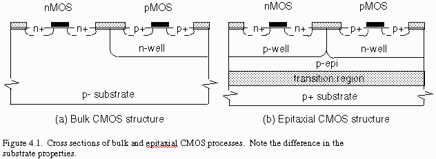
The relative importance of SEE phenomena also depends on circuit fabrication technology. It is not possible to cover all aspects of circuit fabrication, but several generalizations can be made. The two approaches that are used to fabricate most CMOS circuits are shown in Figure 1. Note that both processes rely on a reverse-biased junction to electrically isolate the well and substrate regions.
A large number of integrated circuits are fabricated with bulk substrates because of the low starting material cost. With a bulk substrate, junctions that are diffused directly into the substrate have a very long charge collection path for charge generated by heavy ions within the substrate. This affects both the prompt and diffusion components of the charge-collection process. In general, devices fabricated on bulk substrates are highly susceptible to SEU. Bulk CMOS circuits are often very susceptible to latchup as well.
The second is junction-isolation using an epitaxial substrate. This process begins with a highly doped low-resistivity substrate. A thin (5-15 µm) epitaxial layer is grown on the wafer prior to subsequent processing, and the active circuit elements are fabricated above (and within) the epitaxial layer. The low-resistivity substrate has the effect of limiting the prompt charge collection region to that of the thin epitaxial layer, with the result that much less charge is collected for epitaxial than for bulk processes, raising the minimum LET required for upset-related effects. Epitaxial substrates also improve latchup hardness compared with bulk processes. However, latchup is still possible with epitaxial processes,[3] particularly for scaled technologies.
Newer processes are available that isolate different regions with special oxide layers instead of junction isolation. These processes are costly, but can be very effective in hardening devices to SEE effects. With oxide isolation, the charge collection depth is limited to that of the top semiconductor epitaxial layer because of the underlying oxide. In most cases oxide-isolated circuits are also immune to latchup because they eliminate the possibility of four-layer paths. Oxide-isolated technologies include a technique that forms the isolation region by oxygen implantation (SIMOX),[4] and an approach that bonds two wafers with an oxide separation region, etching one wafer to form a thin epitaxial region (BESOI).[5]
Circuit design and feature size are also important in determining SEE sensitivity. In general, SEE sensitivity increases as devices are scaled to smaller feature sizes. Most scaled devices have faster response times, with lower critical charge. Newer technologies with reduced supply voltage are expected to be even more sensitive because switching levels are reduced, lowering critical charge compared to circuits with higher voltages.
Single-event upset occurs in storage elements when the charge collected from a heavy-ion interaction exceeds the critical charge required to upset the circuit. The circuit then changes state, and stored information is lost. However, the circuit still functions normally, and it can be restored to its original operating state by rewriting or reinitializing the circuit.
Originally, only heavy ions caused single-event upset. However, as individual transistors were scaled to smaller dimensions to increase the size and complexity of VLSI circuits, their sensitivity to SEU increased sufficiently so that it was possible for protons to induce upset as well.[6] This may increase the upset rate by several orders of magnitude because of the large number of protons in solar flares and trapped radiation belts.
In some bulk device technologies multiple-bit upset can occur because of diffused charge in the substrate, which can be collected by several different circuit elements. Devices that are most likely to undergo MBU include DRAMs and four-transistor SRAMs, where diffused charge can be an important part of the charge collection and switching process. MBU can cause the SEU cross section to increase significantly at higher LET values rather than saturating.[7]
Latchup
Most junction-isolated circuits contain parasitic bipolar transistors that can form a four-layer region, similar to that of a silicon-controlled rectifier. These bipolar structures are not involved in normal operation of CMOS devices, but can be triggered by transient currents. Figure 2 shows the bipolar structures that create a four-layer latchable structure in a p-well CMOS circuit. Latchup disrupts normal operation in the region of the circuit where it occurs, causing partial loss of functionality as well as higher current in the local region where latchup occurs.
All CMOS designs use special guardbands and clamp circuits at input/output terminals to prevent latchup from occurring in standard circuit applications. However, in a radiation environment transient signals are no longer confined to I/O terminals, and it is possible for the current pulses from heavy ions or protons to trigger latchup in internal region of a CMOS device, as well as in I/O circuitry.
Once latchup occurs, the four-region structure will be switched into a conducting mode, and it will remain in that mode until power is removed, or until the voltage across the latched region is reduced to very low values. During latchup currents can be very high. In most circuits, currents of several hundred milliamps or more will flow in the localized region where latchup is triggered, rapidly heating that region to extremely high temperatures. These high temperatures not only introduce the possibility of localized damage to the silicon and metallizations, but the excessive heating may also cause the latchup to spread to other regions.
Because of the potential for catastrophic damage, latchup is a very serious problem for space systems. The most conservative approach rules out use of any latchup susceptible circuit. A number of methods have also been proposed to overcome latchup at the system or subsystem level by sensing excess current, which is a signature of latchup, and temporarily removing power. However, power must be removed within a few milliseconds after latchup occurs to avoid possible catastrophic damage. It is also difficult to make sure that latchup detection circuits will be completely effective because many different latchup paths exist in complex circuits, with different current signatures.[8] Device scaling generally increases susceptibility to latchup, and latchup is expected to be even more important for devices with reduced power supply voltage and operating power.[9]
Unlike most radiation phenomena, latchup is highly sensitive to temperature. The threshold LET for latchup is reduced by approximately a factor of three at 125 °C compared to room temperature. [10,11] The larger number of ions with lower LET values in the distribution of galactic cosmic rays [see Sections 3 and 8] causes a factor of three reduction in LET threshold to increase the total upset rate by much larger values at high temperature. Because of this, testing for latchup should always be done at the highest temperature expected in the application.
Snapback
As device dimensions are reduced, the parasitic bipolar transistor within an MOS device has sufficient gain so that its parameters can also affect device operation. Snapback is a reduction in the breakdown voltage of this parasitic transistor that is caused by injection of minority carriers from the source diffusion to the well.[12] Just like latchup, snapback also causes local loss of functional operation, along with an increase in current. However, much smaller currents generally occur as a result of snapback.
Another difference between latchup and snapback is that it is usually possible to recover from snapback by sequencing electrical signals without reducing the supply voltage. Snapback involves only three semiconductor regions, and can occur in oxide-isolated structures as well as in those with junction isolation. Unlike latchup, snapback is not very sensitive to temperature. [13]
As devices are scaled to smaller dimensions, it becomes possible to cause catastrophic damage from the interaction of one (or a small number, i.e. 2-3) ions. These effects have been recently observed in 4 Mbit DRAMs with feature sizes of 0.6-0.8 µm, and are expected to become more important as devices are scaled further.
One mechanism, microdose deposition, differs from other SEE effects in that it involves charge deposition within the gate oxide.[14] This is the same mechanism that causes total dose damage. It becomes significant when the gate area is comparable to that of the microdose deposition region from a single ion. The microdose effect changes the threshold voltage of an individual transistor within a VLSI circuit, increasing the leakage current. This can cause failure in some types of circuits, particularly DRAMs and SRAMs that use a four-transistor memory cell.
The other mechanism appears to be similar to gate rupture in power MOSFETs, and causes a short in the gate region of an individual transistor.[15] This mechanism is important for random logic as well as for memory cells. A similar effect has been seen in field-programmable gate arrays; in this case the heavy ion permanently alters the gate array.[16]
Both mechanisms have been observed for 4- and 16- Mbit DRAMs, but the probability of either phenomenon occurring in space is sufficiently low that neither is very significant for today�s circuit technology. However, both mechanisms are expected to be increasingly important as devices are scaled to smaller dimensions because the threshold LET is expected to decrease.[17]
Heavy-ion tests are done using high-energy accelerators such as the Brookhaven Van de Graaff accelerator or UC Berkeley cyclotron. The range of the particles is very limited -- far less than that of galactic cosmic rays -- and testing must be done within a vacuum chamber. The limited range of the particles can be important when test results are related to space environments, particularly for device technologies where charge diffusion is important. The finite range also means that the LET value changes as the beam passes through the device.
Tests are done using several different ion species, covering a range of LET values. A scattering foil is generally employed within the vacuum system to increase the beam area. The facility is calibrated by measuring the flux rate or current, and by using surface-barrier detectors to determine the LET. During testing, it is important to restrict the total fluence of heavy ions in order to keep from damaging the device that is being tested.[18]Total dose damage and displacement damage can alter device characteristics, affecting SEE test results.
In order to allow a wider range of LET values with fewer ions, it is common practice to adjust the incident angle of the particle beam by rotating the device under test. For a thin p-n junction with constant LET through its depth, the path length increases as 1/cos theta, where theta is the incident angle. This does not change the LET of the ion, but it increase the path length by the secant of the angle. Thus, as long as these assumptions hold, the effective LET increases. Unfortunately this "cosine law" is not always applicable. It fails in several cases: (1) where charge collection occurs over a path length that is a sizable fraction of the total range of the particle (the LET varies along the path); (2) for devices that collect much of their charge by diffusion, where the collection volume is spherical, and the LET does not vary with angle; and (3) where the aspect ratio of the collection volume is small, causing a more complex angular dependence. The validity of the cosine law must be carefully checked for each device technology. Test results should always include angle and range data for each ion species.
Proton tests are also done at accelerators. Unlike heavy-ion accelerators, protons have large ranges, making testing more straightforward. Different reactions are possible for different proton energies. Proton tests are generally done at several proton energies in order to determine the threshold energy level for proton upset instead of threshold LET, which is used for heavy ions.
It is also possible to use californium fission sources for SEE testing.[19] Fission sources are very low in cost, and can be used in a normal laboratory environment. Fission sources produce a spectrum of fission fragment energies, which complicates interpretation of the results. The range of fission fragments is smaller than that of most heavy-ion sources, and this places a major restriction on testing with californium sources. However, californium can be an effective low-cost alternative for technologies with shallow charge collection structures.
Because of the finite range, the effective LET of californium fission fragments decreases rapidly as they go through the device structure. The maximum LET available from californium is approximately 40 MeV-cm2/mg near the device surface. However, this decreases to 10-15 MeV-cm2/mg at a depth of 10 µm. The effective LET of ions from californium depends on the average LET within the charge collection depth, and is usually much less than maximum LET. This needs to be taken into account when californium test results are compared with conventional heavy ion testing; in most cases the saturation cross section with californium is lower than the saturation cross section obtained with heavy ions because of the limited range.
Single-event testing is relatively straightforward for memory circuits, which are often used as an example of single-event testing. It is easy to define the internal conditions and to test the entire storage array of a memory circuit, although large commercial memories may use more complex "hidden" architectures that complicate the interpretation of memory test results.
As discussed in the previous section, testing is done using several different ions (and often several incident angles), measuring the number of errors and the total particle fluence to determine the cross section at various LET values.[20] The error rate must be low enough to avoid complications from multiple errors during short time periods (note that this differs from multiple-bit errors) and to correct for the latency period during the time that the memory is being rewritten.
In all SEE testing, it is important to recognize the importance of counting statistics. Counting uncertainties depend upon the square root of the number of occurrences. In general, at least 100 events should be observed at each effective LET value, and the uncertainty in counting statistics should be included when reporting data. Note that the observance of one or two events is virtually impossible to interpret.
Other VLSI devices, such as microprocessors and random logic are much more difficult to test. Bias conditions play a major role in single-event upset testing, particularly for complex circuits. In order to interpret results, one must know which regions of a device involve internal storage cells, and how many of them are being exercised during the test. For example, test results for some types of microprocessors have shown an order of magnitude increase in cross section when the device is exercised by operations that use cache memory compared to non-cache results.[21]
Many circuit variables affect latchup testing, including the bias conditions applied during testing. Latchup tests should be made under conditions of maximum power supply voltage. As discussed earlier, testing should also be done at the maximum temperature expected in the application. Note that a null result at room temperature means nothing about latchup susceptibility at higher temperature.
Because latchup is a relatively slow process, diffused charge is extremely important during latchup testing. It is important that particles have sufficient range. For devices with p-substrates, charge collection can occur at depths of 60 µm or more. Varying the incident angle may actually lower the adjusted latchup cross section if ions are used with insufficient range.
In most cases a power monitoring and control circuit is used during latchup testing that allows power to be shut down quickly after latchup is detected. If power cycling occurs, care must be taken to account for the "dead time" between shutdown and power up when the latchup cross section is evaluated.
Although latchup usually produces large increases in power supply current, some circuits exhibit very small changes in current ("microlatches"). These microlatches may be caused by localized latchup paths which have relatively high resistance paths (this can depend on the location of the latchup region relative to bond wires and power supply or ground metallization) or by other effects, such as snapback. In many cases insufficient resources are available to distinguish the exact mechanism. Nevertheless, it is important to realize that microlatches can occur and to set up a testing approach that can detect them.
Calculations of SEE rates involves three different quantities:[22,23]
(1) The cross section of the device, often determined empirically;
(2) The distribution of particles expected in the space environment, which depends on assumptions about solar flare activity, radiation belt activity, and shielding; and
(3) The critical charge, sensitive area and sensitive volume associated with the SEE phenomenon of interest.
These three quantities are folded together in order to calculate the estimate of the upset rate. All three are complex, and usually a number of simplifying assumptions are made in the process of doing the calculations. Assuming that the cross section is accurately known, the approach used is outlines below.
Particle Distribution. The particle distribution of galactic cosmic rays is often assumed to follow the so-called Heinrich curve, which provides several distributions of flux vs. LET corresponding to solar max, solar min, a 10% worst-case flare (i.e., only 10% of the expected solar flares will exceed this distribution), and a worst-case flare distribution [this is discussed in more detail in Section 8]. The worst-case distribution is rarely used, because it is not only statistically unlikely but also increases the particle distribution envelope by nearly five orders of magnitude.
Other particle distributions must be added to the distribution of the Heinrich flux. Particles trapped within radiation belts also have a distribution of energies. However, they generally have lower energy than galactic cosmic ray, and are more affected by shielding.
Sensitive Geometry and Critical Charge
The sensitive geometry and critical charge are the most difficult parameters to determine. Charge funneling, which extends the collection depth below the depletion region cannot be determined directly, and involves an assumption about device geometry. For processes where diffused charge is important, it can be even more difficult to determine the appropriate volume for charge collection.
Charge collection assumptions are more straightforward for epitaxial processes, where it is usually reasonable to assume that the charge collection depth is limited by the epi thickness. The effective area for charge collection may be difficult to determine accurately, particularly for cases where the cross section does not saturate, but continues to increase at higher LET values.
Chord-Length Distribution. A cosmic ray can strike an IC from any angle. In order to calculate the number of upsets that will occur, it is necessary to take into account the way that particles intercept the total change collection volume as they pass through it with different locations and angles. These details have been worked out for simple parallelepiped geometries, and can be used to provide a distribution of chord lengths within the volume. [24] The chord-length integral is then used along with the ion distribution and critical charge to determine the probability that particles in the environment will produce an upset.
Error-Rate Prediction Techniques
For cases where a single device geometry is involved, computer programs such as CRUP or CREME can be used to calculate the final error rate, in errors/bit-day. However, these computer codes require a fixed, single value for critical charge and the device collection volume. In real devices the collection volume may depend on LET, complicating the analysis.
It is important to realize that these are very complex calculations, involving many assumptions and uncertainties.[23,24] The result is only an estimate of the upset rate expected in the application. The established approaches work reasonably well for devices with a nearly ideal cross section and sensitive volume, but are less successful for highly scaled devices or for processes involving diffused charge, such as latchup.
Figure 3 illustrates the way that the cross section, particle LET distribution, and sensitive volume are combined to calculate the error rate. Some important details associated with these parameters are discussed below.
The results of these calculations can be expressed in several different ways. One common approach
is to calculate the number of errors that occur in a 24-hour period; this can either be reported for the
entire chip, or normalized to the number of bits, i.e., errors/bit-day. Often two calculations are done,
one for the typical galactic cosmic ray environment, and one assuming a large solar flare. This
provides an approximate estimate of the likely change in upset rate during enhanced solar activity.
Another important factor in error rate calculations is shielding, particularly for lower energy solar
particles and protons in the radiation belts. Although shielding is not discussed here, it often reduces
the error rate to much lower values for devices that are shielded by other equipment or structures
within the spacecraft.
This section of the document provides a brief summary of basic SEE effects. The primary emphasis
was on SEE effects in integrated circuits. Two important areas were omitted because of space
limitations: catastrophic failure in power devices, including burnout in bipolar transistors and gate
rupture in power MOSFETs; and single-event transients in integrated circuits.
It is important to distinguish between transient SEE effects, which are generally easy to recover from,
and catastrophic effects, which are generally of far more concern for most space systems. As devices
are scaled to smaller dimensions, it is likely that catastrophic effects will become increasingly important,
and the success of future space missions may ultimately depend on how well these phenomena are
understood and characterized for various technologies.
Finally, it is important to realize that error rate calculations are complex, and involve many assumptions,
particularly about device geometry. Although error rates for individual components are important, they
are only part of the equation. Other sections of the document deal with ways to accommodate SEE
effects, and one should keep in mind that the net effect of errors on the spacecraft is highly system dependent.
§ Even though the main energy loss mechanism for protons is ionization,
the charge produced by direct ionization from protons is too small to cause SEE effects in most
semiconductors. SEE effects from protons are caused by the reaction products of proton-induced
nuclear reactions.
1. F. B. McLean and T. R. Oldham, "Charge Funneling in n- and p-Type Substrates," IEEE
Trans. Nucl. Sci., NS-29, 2018 (1982).
2. P. E. Dodd, F. W. Sexton, and P. S. Winokur, "Three-Dimensional Simulation of Charge Collection
and Multiple-Bit Upset in Si Devices," , IEEE Trans. Nucl. Sci., NS-41, 2005 (1994).
3. T. Chapuis, H. Constans-Erems, and L. Rozier, "Latchup on CMOS/EPI Devices," IEEE
Trans. Nucl. Sci., NS-37, 1839 (1990).
4. J. T. Shott and W. M. Shedd, "Silicon on Insulator Technologies - Are We Converging On a
Technique of Choice?," IEEE Trans. Nucl. Sci., NS-33, 1366 (1986).
5. W. M. Huang, et al., "ULSI-Quality Gate Oxide on Thin-Film-Silicon-on-Insulator," 1993
IEDM Technical Digest, p. 735.
6. C. S. Guenzer, et al., "Single Event Upsets in RAMS Induced by Protons at 4.2 GeV and Protons
and Neutrons Below 100 MeV," IEEE Trans. Nucl. Sci., NS-27, 1485 (1980).
7. J. A. Zoutendyk, et al., "Empirical Modeling of Single-Event Upset in NMOS Depletion-Mode-Load
Static SRAM Chips," IEEE Trans. Nucl. Sci., NS-33, 1581 (1986).
8. A. H. Johnston and B. W. Hughlock, "Latchup in CMOS From Heavy Particles," IEEE
Trans. Nucl. Sci., NS-37, 1886 (1990).
9. A. H. Johnston, "The Influence of VLSI Technology Evolution on Radiation-Induced Latchup in
Space Systems," accepted for publication in IEEE Trans. on Nucl. Sci., April, 1996.
10. W. A. Kolasinski, et al., "The Effect of Elevated Temperature on Latchup and Bit Errors in
CMOS Devices," IEEE Trans. Nucl. Sci., NS-33, 1605 (1986).
11. A. H. Johnston, B. W. Hughlock, and R. E. Plaag, "The Effect of Temperature on Single-Particle
Latchup," IEEE Trans. Nucl. Sci., NS-38, 1435 (1991).
12. A. Ochoa, et al., "Snapback: A Stable Regenerative Breakdown Mode of MOS Devices,"
IEEE Trans. Nucl. Sci., NS-30, 4127 (1983).
13. R. Koga and W. A. Kolasinski, "Heavy-Ion Induced Snapback in CMOS Devices," IEEE
Trans. Nucl. Sci., NS-36, 2367 (1989).
14. T. R. Oldham, et al., "Total Dose Failures in Advanced Electronics from Single Ions,"
IEEE Trans. Nucl. Sci., NS-40, 1820 (1993).
15. G. M. Swift, D. J. Padgett, and A. H. Johnston, "A New Class of Single-Event Hard Errors,"
IEEE Trans. Nucl. Sci., NS-41, 2043 (1994).
16. R. B. Katz, and G. M. Swift, "Data on Anti-fuse/FPGA Reliability in the Heavy-Ion Environment,"
presented at the IEEE Nuclear and Space Radiation Effects Conference, Madison, WI, July, 1995; submitted
for publication in the IEEE Transactions on Nuclear Science.
17. A. H. Johnston, G. M. Swift, and D. C. Shaw, "Impact of CMOS Scaling on Single-Event Hard
Errors in Space Systems," Digest of Technical Papers, 1995 IEEE Symposium on Low Power
Electronics, p. 88, October, 1995 (IEEE Pub. 95TH8138).
18. F. W. Sexton, "Measurement of Single Event Phenomena in Devices and ICs," Chapter 3
of Short Course Notes from the IEEE Nuclear and Space Radiation Effects Conference, New Orleans, LA, July, 1992.
19. J. T. Blandford and J. C. Pickel, "Use of Cf-252 to Determine Parameters for SEU Rate
Calculations," IEEE Trans. Nucl. Sci., NS-32, 4282 (1985).
20. K. A. LaBel, et al., "Single Event Effect Proton and Heavy Ion Test Results for Space Electronics,"
1994 Radiation Effects Data Workshop, p. 64 (IEEE Pub. 94TH06841).
21. R. Velazco, S. Karoui, and T. Chapuis, "SEU Testing of 32-Bit Microprocessors," 1992 IEEE
Radiation Effects Data Workshop, p. 16 (IEEE Pub. 92TH0507-4).
22. E. L. Petersen, et al., "Rate Prediction for Single-Event Effects -- A Critique," IEEE Trans.
Nucl. Sci., NS-39, 1577 (1992).
23. L. W. Massengill, "SEU Modeling and Prediction Techniques," Chapter 3 of Short Course
Notes from the IEEE Nuclear and Space Radiation Effects Conference, Snowbird, UT, July, 1993.
24. W. G. Abdel-Kader, et al., "Estimating the Dimensions of the SEU Sensitive Volume," IEEE
Trans. Nucl. Sci., NS-34, 1300 (1987).
Introduction4.4 Summary
Notes
![]()
4.5 References
![]()
1. The SEE Problem
2. Functional Analysis and Criticality
3. Ionizing Radiation Environment Concerns
4. Effects in Electronic Devices and SEE Rates
5. SEU Propagation Analysis: System Level Effects
6. SEE Mitigation: Methods of Reducing SEE Impacts
7. Managing SEEs: System Level Planning
8. SEE Criticality Assessment Case Studies